| thinfilmmfg.com
|
IMEC's annual research review meeting, held two weeks ago in Leuven, Belgium, surveyed the institute's new and ongoing projects. As the largest independent microelectronics research and development center in Europe, IMEC's research partners include a wide range of electronics manufacturers and their suppliers. Areas of interest range from the leading edge of current manufacturing to the distant horizon of the semiconductor industry's Technology Roadmap.
This year, the review meeting highlighted projects in three major areas:
Near term projects include a 100 nm CMOS program, in collaboration with Phillips Research. According to Malgorzata Jurczak of IMEC, the project began by developing core modules for 100 nm CMOS, such as the gate stack, shallow trench isolation, and ultrashallow junctions. In the now-completed device optimization phase, researchers found that rapid thermal nitridation of the SiO2 gate dielectric can reduce gate leakage by two orders of magnitude. Optimization of source/drain extensions can have a similar impact. Since gate leakage limits the transistor off current, and therefore its power consumption, these optimizations are essential for scaling low power devices down to the 100 nm technology node. The next phase in the project will combine transistors with an interconnect process for full system integration.
At the 70 nm node, the interconnect process will also require significant changes, IMEC Fellow Karen Maex explained. According to the Roadmap, the interlayer dielectric will need to offer a dielectric constant (k) of 2 or less. All known candidate materials, both spin-coated and chemical vapor-deposited, are porous. Process engineers will have to confront an enormous range of challenges--including hard mask deposition, patterning, cleaning, and integration with copper damascene processing--without degrading the k value, reliability, or manufacturability of the dielectric. Maex warned that many diffusion barriers will penetrate porous dielectrics, either by diffusion or by deposition on the pore walls. Pore size and connectivity must be designed with barrier compatibility in mind. She suggested that the barrier layer should actually be seen as a nanolaminate, including a low-k adhesion layer, the diffusion barrier itself, and a copper adhesion layer.
According to VP Luc Van den hove, IMEC's three-year old 193 nm lithography project is also bearing fruit. The research group has printed 70 nm gates using 193 nm lithography with both scattering-bar enhanced binary masks and alternating phase shift masks. The alt-PSM masks offer a larger process window, allowing both 100 nm and 70 nm isolated lines to print under the same exposure conditions.
The IMEC group used fewer optical "tricks" than are normally needed so far below the exposure wavelength. Researchers were able to print 100 nm gates using normal binary masks, without optical proximity correction and with conventional illumination. Van den hove explained that the most advanced photoresists have improved dry etch resistance, are less prone to pattern collapse, and are less susceptible to line edge roughness. As a result, less aggressive resolution enhancement techniques can be used.
Though these advances increase the size of the process window, exposure latitude is still very low compared to previous lithography generations. Van den hove expects that advanced process control will be critical for manufacturability of sub-100 nm features.
Looking further into the future, IMEC has two projects devoted to sub-45 nm device designs. One will focus on silicon-compatible transistors below 45 nm gate lengths. According to Kristin De Meyer, this three-year program will concentrate on identifying the limits of conventional CMOS, including integration issues for high-k gate dielectrics and ultrashallow junctions. In addition to device demonstrations, the project will try to develop quantum-mechanical simulation models and nanometer-scale materials characterization techniques.
A closely related project will study non-bulk CMOS device architectures such as double-gate devices, strained Si/SiGe structures, and fully-depleted silicon-on-insulator (SOI). This project, De Meyer said, will be especially interested in easing the transition to the post-CMOS era, for instance by ensuring compatibility between new architectures and existing process technologies.
New transistor materials often require new package designs. For example, the reduced hardness of low-k dielectrics substantially alters package mechanics. At the review meeting, IMEC announced a new Industrial Affiliation Program focused on packaging for integrated circuits using copper and low-k dielectrics.
|
Click image for larger version. Source: IMEC. |
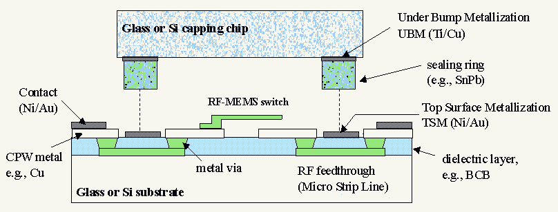
Other emerging devices will require unique packages as well. As Kris Baert of IMEC's Microsystems, Components, and Packaging Division explained, microelectromechanical systems (MEMS) implement non-electrical functions. They interact with their environments in very different ways from integrated circuits. Baert described what IMEC claims is the world's first wafer-level package for a MEMS RF switch. Besides meeting typical IC packaging requirements, the RF-MEMS package protects the mechanical switch from damage and contamination, while maintaining a controlled ambient around the switch. |
Ideally, designers would like to manufacture MEMS devices and their CMOS control logic simultaneously. Pre-processing--manufacturing the MEMS devices before transistor formation--allows high temperature MEMS processes but exposes the mechanical devices to all the rigors of the CMOS process sequence. Post-metallization processing has little or no impact on the CMOS manufacturing sequence, but limits the MEMS processes to temperatures below 400 or 450°C. Modifying the CMOS interconnect process to include MEMS devices imposes a thermal budget due to the risk of dopant diffusion, but may ultimately be the most flexible approach.
More conventional RF devices can benefit from advanced packaging as well. Walter De Raedt described an RF system-in-package (SIP) approach. Integrating active and passive components on a single substrate reduces total system size for wireless portable applications. At the same time, package-level integration eliminates many of the costs and complexities associated with system-on-chip (SOC) designs.
An SIP package must minimize parasitic effects, both in the chip/substrate interconnection and in the connection between the package and the system board. IMEC's approach uses an MCM-D technology, modified for microwave systems. A glass substrate supports three metal planes. The design can accomodate coplanar waveguides and other passive devices, with either flip-chip or wire bond connections to the IC. The approach is fully compatible with the RF-MEMS package discussed above.
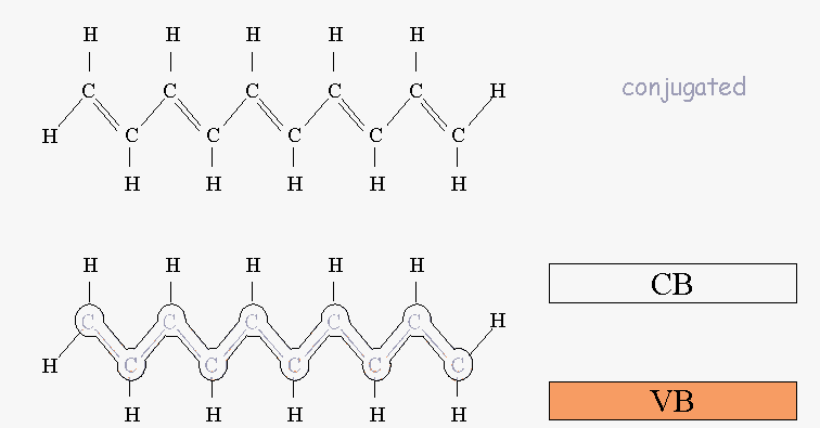
| Not all of IMEC's activities offer such near-term benefits. Paul Heremans discussed the institute's work on plastic electronics. Semiconducting plastics are typically conjugated molecules. Carbon atoms in the molecular backbone bond with three nearest neighbors, leaving a fourth electron free to carry current. Inexpensive and flexible, plastic substrates are attractive for disposable and large-area applications like displays and solar cells. IMEC is collaborating with Belgian universities to improve understanding and synthesis of these materials. |
Click on image for larger version. Source: IMEC |
Semiconducting plastics include both polymers and smaller molecules. Polymers are typically solution-processed, leading to relatively high impurity levels. Composition and molecular weight for polymers vary around a statistical mean. IMEC's research focuses on smaller molecules like pentacene and perylene. These can be purified by sublimation, have precisely defined compositions and molecular weights, and can be deposited by vacuum methods. According to Heremans, IMEC's research on plastic electronics focuses on improving material and device properties while reducing the cost of manufacturing. Fabrication techniques for semiconducting polymers are quite different from the familiar CMOS processes. Inkjet printing, solid ink printing, and self-assembled monolayers are all being considered.
Still further out on the leading edge, Jo De Boeck discussed nanometer-scale devices. Behavior of these devices is dominated by quantum effects. In spin-tunnel junctions, for example, an oxide layer separates two magnetic layers. If the majority spins in the two magnetic layers are aligned, electrons can tunnel through the oxide with relatively little resistance. If the spins are opposite, resistance through the junction jumps by 40-50%. Spin-based devices are aleady used in magnetic sensors for hard disk drives. Novel "spintronic" devices may also have applications in quantum computing and in electro-optical devices. Magnetic semiconductors may also be possible: GaN and InN have Curie temperatures near room temperature. IMEC's spintronic research, funded by the European Community, is particularly interested in magnetic semiconductors and spin-injection for tunnelling devices.
More than half of IMEC's contract research is funded by the international microelectronics industry. The organization expects revenue to grow 20% in 2001, president and CEO Gilbert Declerck said. It is not immune from the global slowdown, however, and expects small growth in 2002. Though many company research budgets are shrinking, reduced resources encourage companies to leverage their research budgets through organizations like IMEC. In Declerck's view, shared research will be essential as the semiconductor industry faces the challenges of the sub-100 nm era.
| This site is Copyright ©2001 by Thin Film Manufacturing. All Rights Reserved |