| thinfilmmfg.com
|
23 July 2001
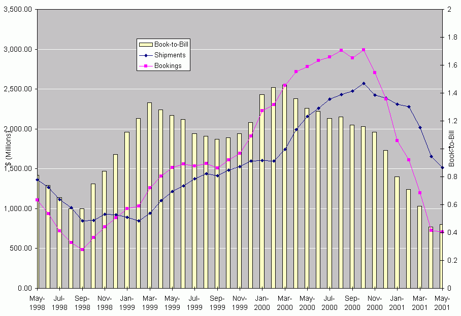
The business news out of Semicon West, held last week in San Francisco (wafer processing) and San Jose (test, assembly, and packaging), was uniformly bad. Though the drop in semiconductor equipment orders leveled off in May (see chart), SEMI members dont think the bottom is in yet. About 60% of members surveyed expect the order trough will be reached in the third or fourth quarter of 2001, with most of the rest placing the bottom in 2002. Of the top ten capital spenders, only Intel, Infineon, and Micron are expected to spend more in 2001 than in 2000.
Foundry fab utilization recently plunged to record low levels, with Chartered Semiconductor using only 31% of its capacity in the quarter ended June 30. For the first quarter of 2001, SEMI estimated the integrated circuit industrys unused capacity at more than 200,000 wafer starts per week.
The only bright spot, mainland Chinas equipment market, is expected to reach US$4 billion this year, and US$7 billion by 2003. That pace is well ahead of last years estimates, which expected the $4 billion milestone would be reached in 2003.
As of July 1, nearly 200 exhibitor companies had chosen to skip the San Francisco show entirely, with only 1,001 registered exhibitors compared to last years total of 1,180. Attendee registration was similarly anemic. As of July 1, the combined San Francisco and San Jose shows had only 45,554 attendees registered, including exhibitor personnel, compared to last years actual attendance of 67,729.
Despite the gloomy outlook, Moores Law continues its steady march toward smaller, faster transistors. When business is bad, the focus shifts to the technology engines that will put the equipment business back on its feet.
In recent years, the transistors themselves have been a major technological concern. The International Technology Roadmap for Semiconductors (2000 update) calls for drain extension junction depths to reach 20-35 nm by 2004 (the 90 nm technology node). According to the Roadmap, no known solutions yet exist for such shallow junctions. Even the less aggressive junctions required by the 130 nm technology node remain problematic.
As Dick Aurelio, chairman and CEO of Varian Semiconductor, explained ultrashallow junctions present two technical problems: placing the dopant in the desired location, and keeping it there during thermal activation. Varian thinks it has solved the first problem with its P2LAD pulsed-plasma system. Aurelio explained that conventional ion implant systems, faced with shallow junction depths, use low energy beams and implant only a few ions per unit time. Since shallow junctions also require relatively high dopant doses (sheet resistance of 220-650 ohms/sq. at the 90 nm node), these systems tend to be very slow. Dose and energy uniformity are also difficult to control with a low energy beam. The P2LAD system, in contrast, immerses the wafer in a dopant-containing plasma. The beam is inherently uniform and conformal, with perpendicular ion trajectories.
For solutions to the second problem, keeping dopants in place, Varian formed an alliance with Ultratech Stepper and Tokyo Electron Ltd. Ultratech chairman and CEO Art Zafiropoulo explained that his companys Verdant Technologies division focuses on laser annealing for ultrashallow junctions. Laser thermal processing (LTP) actually melts the surface of the wafer, achieving more complete dopant activation than is possible by conventional means. At the same time, the extremely rapid processing prevents dopant diffusion, maintaining steep junction profiles.
Tokyo Electron is involved in the project because a third technical issue arises as a side effect of LTP. Molten silicon flows, smoothing out intentional topography like gate structures. A thin PVD cap layer is needed to protect device structures during the laser processing step. Susan Felch, director of Varians research center, said that several different cap materials are being considered, including TiN and other materials currently used as diffusion barriers.
The three companies are building a 20,000 ft2 Advanced Technology Center in San Jose, California, near Ultratechs corporate campus. The center, scheduled for completion by the end of this year, will focus on process development. The partners have not yet decided to extend their agreement to joint marketing of equipment.
Dow Chemical also sought safety in numbers with its SiLKnet alliance. The alliance, which includes nine different suppliers of cleaning, CMP, and etch processes for Dows SiLK dielectric resin, will share a pool of blank and partially processed wafers. Members can use those wafers for process integration and equipment and materials development. Current generation SiLK materials offer a dielectric constant (k) of 2.6, with porous materials in the k = 2.0 range under development.
Meanwhile, Dow Corning, a joint venture of Dow Chemical and Corning, offers a confusingly named XLK series of dielectric resins with k values between 2.0 and 2.5. The material, based on hydrogen silsesquioxane (HSQ), is deposited by spin-coating. A brief wet ammonia treatment causes gelation, then a brief bake at 150°C evaporates solvents and creates pores. An oxygen-free plasma cure crosslinks the remaining HSQ resin for structural stability. The company reports that the dielectric constant of the material depends on the density of pore walls, not on the degree of porosity. As a result, a single process integration scheme should continue to work across the full range of k values.
According to Michael D. Little, Dow Cornings business director for semiconductor fabrication materials, the company is embroiled in patent litigation against Tokyo Ohka Kogyo Co. Ltd. Dow Corning filed suit in the United States last July, alleging infringement of several US Patents covering its HSQ materials and processes:
Last week, the company filed suit in Korea as well, alleging infringement of comparable Korean patents:
Dow Corning is targeting the XLK material for the 100 nm technology node. The company also supplies trimethylsilane precursor gas for CVD dielectrics like Applied Materials Black Diamond. Little expects CVD dielectrics will account for 70% of the market at the 130 nm technology node. It is not clear whether CVD materials are extensible below the 100 nm generation.
The poor business climate has also increased interest in integrated metrology, e-diagnostics, and other productivity improvements. According to Giora Dishon, managing director of Nova Measuring Instruments, many IC manufacturers view standalone metrology tools as a cost, while integrated metrology systems add value. For example, a standalone metrology tool can only indicate a manufacturing problem, while integrated metrology can support real-time process control. Novas film thickness measurement is integrated with Applied Materials Mirra CMP systems. Applieds new Transforma etch system also relies on integrated metrology, using automatic critical dimension measurement for improved control of gate dimensions.
On the e-diagnostics front, domainLogix teamed with AMD and ILS Technology to demonstrate several e-diagnostics products. The e-Centre framework, developed by ILS and domainLogix, supports secure equipment connectivity and remote tool access and troubleshooting. It relies on the object-based equipment model (OBEM) to manage the interface to each individual tool. Applications, such as AMDs ASPECT statistical proces control package, dont need to worry about networking or internal equipment details. Bob Bruck, Intels director of fab capital equipment development, has said that useful e-diagnostics are still three equipment generations away. Richard Deininger, AMDs director of strategic equipment technology planning, disagrees. He said that AMD is using e-diagnostics now, and in fact couldnt make manufacturing changes as quickly as it does without the technology.
Overall, the Semicon West mood was much more optimistic than might have been expected, given the poor business climate and the recent steady drumbeat of gloomy analysis in the business press. Yes, conditions are bad, but the future of electronics applications remains bright. Companies, and individuals, are riding out the storm and preparing for the opportunities that will eventually appear.
| This site is Copyright ©2001 by Thin Film Manufacturing. All Rights Reserved |