| thinfilmmfg.com
|
As transistors shrink, it becomes more and more difficult to meet leakage, drive current, and other performance specifications. High dielectric constant (high k) gate materials, ultrashallow junctions, and other modifications to the conventional MOSFET transistor design have proven very difficult to implement outside the laboratory. Researchers trying to maximize transistor performance are looking further and further afield.
Silicon-on-insulator (SOI) transistors have emerged as one of the leading alternatives. The insulating substrate reduces junction capacitance and improves transistor speed, while requiring few changes to the wafer process. In 1998, IBM announced it would use SOI wafers for its high performance microprocessors. Though Texas Instruments, AMD, and Motorola joined the SOI camp last year, Intel had remained skeptical. Thus, Intel's previously reported announcement that it would use SOI for its 50 nm transistor design was one of the biggest stories of this year's IEEE Electron Device Meeting, held last week in Washington, DC.
As the Intel researchers explained, the silicon layer in an SOI structure can be either partially depleted or fully depleted. Partially-depleted SOI is prone to the floating body effect (FBE), which requires significant changes to the circuit design. Moreover, Intel believes, the performance gains of P-D SOI do not scale as the devices shrink. The work described at IEDM implemented fully-depleted SOI transistors with gate lengths as low as 50 nm and silicon layers less than 30 nm thick. These so-called depleted substrate transistors (DST) avoid the FBE, with better subthreshold slopes and similar CV characteristics compared to bulk Si CMOS transistors. With raised source/drain structures, the DSTs achieved drive current more than 20% better than both partially-depleted SOI and bulk Si transistors.
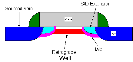
| Such small transistors are prone to the short channel effect, which increases off-state leakage current. Halo doping helps control this effect by creating a steep dopant profile at the edges of the source/drain regions. In bulk Si, halo doping also increases junction capacitance. Samuel Fung and coworkers at IBM showed that thin (45 nm) SOI eliminated this issue. Fung's group demonstrated 36 nm gate length transistors with excellent drive current and intrinsic gate delay. |
Click image for larger version. |
Alternatively, S. Narasimha and coworkers, another IBM group, used a spacer to limit the overlap of the source/drain extensions beneath the gate while maintaining conventional implant doses and thermal cycles. By reducing the overlap, Narasimha's group was able to control short channel effect with moderate halo implant doses.
The physics of such thin-body transistors are not yet well understood. Ken Uchida and coworkers at Toshiba found that quantum mechanical effects are responsible for low carrier mobility, increased gate-channel capacitance, and increased threshold voltage in these devices. Briefly, when the silicon thickness is smaller than the inversion layer thickness of bulk MOSFETs, the structural confinement of the inversion-layer electrons increases the sub-band energy levels.
| This site is Copyright ©2001 by Thin Film Manufacturing. All Rights Reserved |