| thinfilmmfg.com
|
by Bryan Lord, AmberWave Systems, Salem, NH USA
Although the semiconductor industry has fueled the information age, creating massive economic value, several cracks are developing in its underlying fundamentals. Exponentially increasing fab costs, slowing unit demand growth, decreasing prices, and increased competition all indicate that the industry may be facing structural problems. This paper analyzes the industry’s rising capital requirements and deteriorating profitability dynamics, and proposes one possible solution to mitigate these adverse trends.
The payback period on invested capital is approaching an untenable level relative to product lifecycles, driven by the rising capital investment required to keep pace with increasingly complex semiconductor chip designs. A poor industry profit picture, highlighted by soft growth in units and average selling prices (ASPs), suggests that improvement in the payback period must come from a more efficient use of production assets. Extracting more cash profits from a given level of capital investment gives the industry greater potential to compress its capital payback period and improve its underlying economics.
New materials offer one way to extend the useful life of production assets, thereby reducing the need for continual new investment in order to improve chip processing speed. In particular, strained silicon has the potential to drive a 20-30% increase in chip processing power while leveraging existing design and manufacturing infrastructure. Incremental production costs are minimal.
In 1965, Intel founder Gordon Moore predicted that the number of transistors on a microprocessor would double approximately every two years. For the last 35 years, this prediction has held true. The number of transistors per microprocessor has increased approximately 20,000 times, processing speeds have increased over 35,000 times, and DRAM capacities have increased over 200,000 times. The ability to pack more processing power on a single chip has driven down the finished cost of many goods, while at the same time increasing their functionality. Electronic devices that contain semiconductors touch nearly every aspect of our work and personal lives, from PCs and cell phones to microwave ovens, alarm clocks and thermostats. Improvements in semiconductor chip design have made the information revolution possible, creating billions, if not trillions, of dollars of economic value.
Given its central role in defining the rate of progress, the semiconductor industry should exhibit attractive returns on invested capital. Recent trends, however, suggest the opposite is true. Flat industry revenues over the past seven years have been accompanied by a steady increase in capital requirements to build state-of-the-art production facilities.
With capital requirements on the rise and the duration of product lifecycles unchanged at 18-24 months, the semiconductor industry is approaching an untenable situation in which the payback period on invested capital will exceed the productive life of the underlying assets.
This problem, its root causes, and one potential solution are the topics of this article. First, an analysis of the industry’s payback period on invested capital demonstrates that payback periods are lengthening and approaching a potentially unsustainable threshold. Two key reasons for this trend are: i) rising capital investment requirements and ii) deteriorating profitability, driven by a shift from supply to demand constraints, softening unit and ASP growth, rising fixed costs as a proportion of total costs, and increased competition. New materials – specifically strained silicon – offer one potential solution to the industry’s rising capital investment requirements.
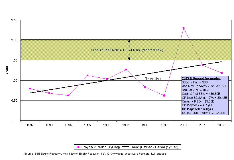
| Over the past ten years, the semiconductor industry’s capital requirements1 have grown faster than its cash operating profits.2 As a result, the payback period on invested capital has nearly doubled, from about 0.7 years to about 1.4 years over that same time period (Refer to Appendix for underlying methodology). Product lifecycles in the industry have remained generally unchanged at 18-24 months, however. Soon, the industry will reach a point at which investment is no longer profitable from a cash net present value (NPV) perspective: the payback period on invested capital will exceed the timeframe over which the underlying assets are productive. |
Net Operating Cash Profit Payback on Invested Capital. Click for larger version. |
The key to understanding why the payback period on invested capital has been rising lies in disaggregating this calculation into its component parts. This analytical framework reveals steadily rising capital investment requirements (producing a higher numerator), coupled with steadily declining profitability (producing a lower denominator), thereby accounting for the increase in the payback ratio over time. Each is considered in turn.
To date, exponential improvements in semiconductor processing power have been made possible only by increasingly complex chip designs that allow manufacturers to pack more and more transistors per square inch. Chip design complexity is the principal driver of rising capital requirements in the semiconductor industry. The equipment and production processes capable of producing chips both with more layers and smaller geometries (reduced line widths and gate sizes) are themselves more complex, and therefore more expensive. The cost of cleanrooms that house the equipment has risen to keep pace with more stringent purity standards required to produce chips with smaller geometries.
|
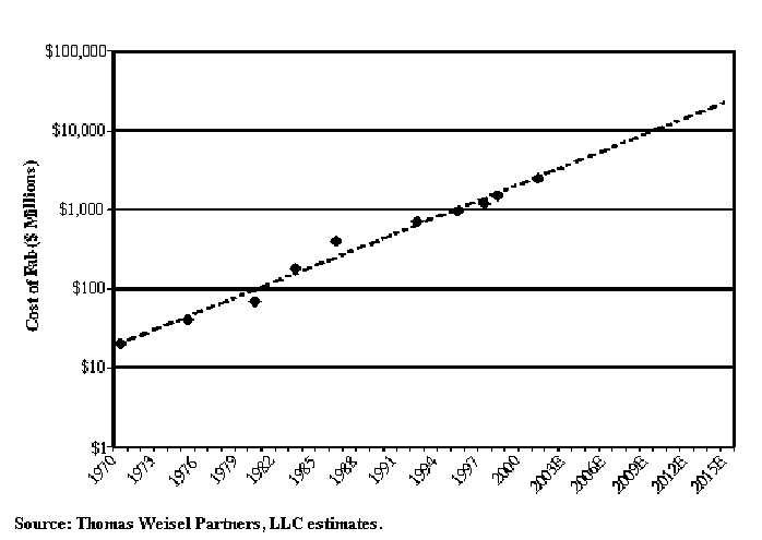
Fab costs expected to continue upward climb. Click for larger version. |
The result has been an exponential increase in the cost of building a chip fab. The cost to build a fab has increased from about $6 million in 1970 to approximately $3 billion for a state-of-the-art 300mm fab in 2002 – a 500-times increase over 30 years. At this rate, fab costs will reach $10 billion by 2007 and $18 billion by 2010.3 |
A combination of factors are contributing to declining profitability in the semiconductor industry, including a secular market shift from supply to demand constraints, softening unit and ASP growth, rising fixed costs as a proportion of total costs, and increased competition. Given their duration (six – seven years), these trends appear to be structural, not cyclical, phenomena.
Market Shift from Supply to Demand Constraints. During the past seven years, the semiconductor industry has shifted from a generally supply-constrained market to a generally demand-constrained market. This shift is significant because industry profitability over the past 35 years has been propelled by reductions in unit costs made possible by economies of scale during a period when industry demand outstripped industry supply. Recently, however, industry demand has slowed to a rate that prevents manufacturers from obtaining lower unit costs on a still rising cost structure. The result is overcapacity, rising unit costs, and increased pricing pressure. In many respects, this transition from supply to demand constraints signifies that the industry is no longer in control of its own profit potential.
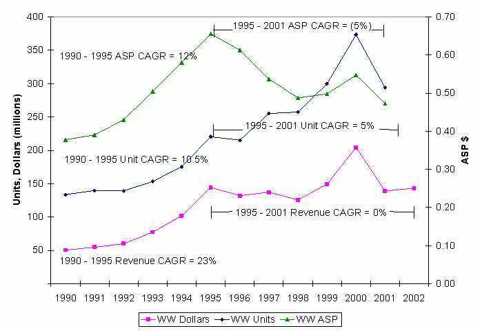
| Softening Unit and ASP growth. Both unit and ASP growth have declined in the seven years since 1995, reflecting this structural shift in demand and supply dynamics. Unit growth declined from 10.5% compound annual growth between 1990 and 1995 to 5% compound annual growth between 1995 and 2001.4 ASP growth declined from 12% compound annual growth between 1990 and 1995 to negative 5% compound annual growth between 1995 and 2001. Both trends show why the industry has been experiencing flat revenues and reflect a secular maturing in industry demand. In turn, maturing demand has produced a condition of oversupply and overcapacity that has forced unit prices to decline more precipitously than unit costs. Over the 1995 to 2001 period, unit facility costs (as measured by IC Knowledge) declined by approximately 38%5 while unit prices (price per transistor, as measured by Intel) declined by about 90%.6 All else being equal, this simple fact suggests shrinking cash profits and a longer payback period on invested capital. |
Revenues, Units & ASP Compound Annual Growth Rates (CAGR) Source: SIA. Click for larger version. |
Rising Fixed Costs as a Proportion of Total Costs. The "stickiness" of unit costs relative to unit prices can be explained by rising fixed costs as a proportion of total costs. Ideally, the semiconductor industry would have a very flexible (i.e. variable) cost structure given the cyclicality of demand. In fact, the opposite is true. From 1992 to 2001, fixed costs per unit7 as a proportion of total unit costs increased from approximately 32% to 42%.8 Rising R&D spending and manufacturing costs fueled this increase. Higher manufacturing costs, in particular, are compounded by the fact that capacity additions are coming on line in progressively larger increments – due to the transition from 200mm to 300mm fabs – exacerbating industry supply/demand imbalances and causing average fab utilizations to decline. For the industry, the implication of this increasingly high fixed cost structure has been a reduction in flexibility to absorb secular slowdowns in demand. In a period of falling prices from 1995 to 2001, fixed costs per unit remained approximately flat. As a result, fixed costs per unitas a percentage of ASPs increased from 36% in 1995 to approximately 50% in 2001,9 sharply compressing cash profits.
Increased Competition. Aside from sluggish demand and rising fixed costs, the backdrop for declining industry profitability has been increased competition, resulting from a disaggregration of the industry’s supply chain. In the semiconductor industry’s early days, a relatively small number of integrated device manufacturers (IDMs) competed with each other at most points in the supply chain. Industry participants included companies such as DEC, Fairchild Semiconductor, IBM, Intel, and Motorola. Over time, some of these players spun-off, or exited, certain parts of their businesses for a variety of reasons, such as rationalization of lower-margin or non-core businesses, a desire to focus on specific areas of expertise, or to raise cash. Teams left the bigger players to form their own companies – typically fabless startups -- focused on a specific need or application. Currently, the greatest area of competition is in the design segment (fabless), where the capital requirement is low and the drive for new designs and products is strong. The result has been an aggregate increase in the number of industry participants, fierce competition for business, and declining prices to finished good manufacturers. This is a positive outcome for businesses and consumers, but a less desirable outcome for industry participants seeking to exert pricing power to drive profitability.
The factors discussed above have created a situation in which the industry has lost broad control over both pricing and demand. Manufacturers must focus on costs and the supply side of the equation to bring both in line with the industry’s new dynamics. In short, manufacturers must reduce the level of capital investment required to produce any given number of chips if they intend to reverse the adverse trend of lengthening payback periods on invested capital. The following points describe why reducing capital investment is a more viable means of improving overall industry economics, rather than trying to improve industry pricing.
Increased Competition Among Design Firms. Scores of fabless design firms now compete to deliver chips with better price/performance characteristics. This dynamic has put foundries in a very difficult position. To keep pace with design innovation, foundries are forced to build new fabs capable of manufacturing chips with smaller geometries. Yet given soft demand, foundries have been unable to attract sufficient volume to produce attractive economies of scale. As a result of this underutilization, unit manufacturing costs have ballooned and cut sharply into foundries’ profits.
Capacity Additions in Larger Increments Exacerbate Problem of Oversupply. In the inevitable move from 200mm to 300mm manufacturing environments, manufacturers obtain 2.5 times more surface area per wafer.10 Fabs capable of handling 300mm wafer platters are the largest ever built. With the size of fabs increasing, the probability of fully utilizing them is declining rapidly – particularly in the face of weak demand – which only magnifies the existing problem of plant underutilization and high unit manufacturing costs. Profits will continue to suffer until manufacturers can find ways to improve capacity utilization by extending the useful life of their production assets.
Longer Product Lifecycles Will Not Materialize. In the past, a doubling of transistors per square inch has corresponded with the start of a new product generation, both happening about every two years. Although Gordon Moore recently commented that the doubling of transistors per square inch will slow from every two years to every four or five years,11 product lifecycles are less likely to follow suit. Competition and innovation among fabless design firms is likely to keep product lifecycles at their current length of 18 to 24 months. Manufacturers must find alternate ways to deliver higher performance chips without resorting to new fabs that can increase the number of transistors per square inch. Accomplishing more with the same, or reduced, capital investment is critical to restoring attractive industry economics.
|
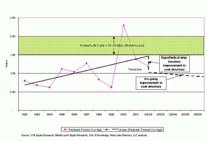
Hypothetical step-function improvement in cost structure. Click for larger version. |
To reduce the current level and pace of capital outlays, the industry must disrupt the present development cycle, whereby advances in chip processing performance are obtained via continual upgrades to the manufacturing base. A shift in production methodology that makes more efficient use of existing installed capital equipment would likely produce a substantive reduction in capital requirements. Ideally, the result would be an immediate, and continuing, reduction in the industry’s payback period on invested capital. |
New materials offer one of the best avenues for extracting more processing power from any given chip design, greatly diminishing the need for continual investment in new production processes to generate incremental performance improvements.
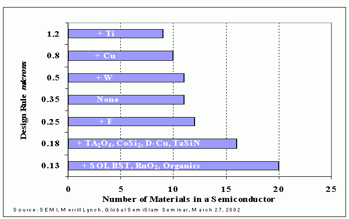
| Materials innovation is not new to the semiconductor industry. Historically, new materials have played an important role in achieving enhanced semiconductor performance. In particular, new materials have been central to the adoption of new production process nodes capable of delivering chips with smaller geometries, more transistors per square inch, and hence enhanced performance. The number of elements found in a fab has increased steadily over time from an original base of just silicon, oxygen and aluminum. |
Number of materials in an integrated circuit. Source: SEMI, Merrill Lynch. Click for larger version. |
Over the past several years, copper has largely supplanted aluminum as the electricity conductor of choice. Optimizing electricity conductivity became a real priority in chip design because resistance and capacitance increase as the metal lines on chips get longer, thinner and closer together to squeeze more transistors per square inch. Given aluminum’s conductive properties, gains in chip speed were diminishing relative to the number of transistors added. Even though copper was more costly, difficult to work with, and required an entirely new manufacturing process, it was adopted because its conductive properties were superior to aluminum’s, thereby reducing resistance and capacitance at smaller chip geometries. Copper made the industry’s move to a new process node feasible and perpetuated the cycle of performance improvement achieved by squeezing more transistors on to a single chip.
Materials additions thus far have facilitated adoption of new production processes, rather than enhancing existing ones. Substrate-layer alternatives to traditional silicon, on the other hand, represent a significant opportunity to increase chip processing speeds without relying on process shifts aimed at squeezing more and more transistors on to a single chip. The ramifications for the industry could be substantial. Chip manufacturers could be positioned to alter the untenable cycle of investment required to keep pace with design improvements and process shifts, thereby improving industry economics and reducing their payback period on invested capital.
Alternate substrate-layer materials can produce faster processing speeds for any given number of transistors, thereby reducing the reliance on process node shifts as the sole determinant of performance improvement. Current options for alternate substrate materials include gallium arsenide, indium phosphide, silicon germanium, silicon on insulator, and strained silicon. Of the several substrate-layer alternatives to traditional silicon, strained silicon currently has the most promise for widespread commercial adoption.
Currently, strained silicon delivers approximately a 20-30% increase in processing speed or reduction in power consumption when using existing chip designs and the process geometries of current fab facilities. The economic impact is to extend the useful life of production assets such that a given level of investment will produe more cash flows. Since strained silicon leverages existing designs and fabs, the only real incremental cost is the increased cost per wafer. For comparative purposes, a traditional 200mm silicon wafer costs approximately $80, while a 200mm strained silicon wafer is projected to cost less than $200,12 only about a two percent increase in total costs per processed chip.
While some alternatives such as gallium arsenide and indium phosphide have superior electron carrier mobility relative to strained silicon, they lack comparable mechanical strength and structural uniformity and require significant new capital investment. These alternatives are ideal for low-volume batch production runs, but not for high-volume applications.
Future generations of strained silicon are expected to continue producing performance gains, leveraging the existing production base. Accordingly, the pace of future capital investment is likely to slow as the useful life of production assets is extended. This development is positive for the industry: greater cash profits can be extracted from a given investment in assets, thereby reducing the payback period on invested capital and enhancing cash returns.
The semiconductor industry has reason to hope that it will not crumble under the weight of its own capital investment requirements. Alternate substrate-layer production materials – strained silicon in particular – offer the industry an opportunity to break the current cycle of generating performance improvement solely through substantial capital investment. The positive impact should be a reduction in the payback period on invested capital and a general improvement in overall industry economics.
AmberWave Systems is the complete commercial source for implementing market-ready strained silicon technologies, allowing customers to bring higher performance devices to market faster and more affordably. Through its work with major semiconductor companies at all points in the supply chain, AmberWave is helping drive adoption of strained silicon, providing the semiconductor industry the fastest, easiest path to its cost and performance enhancements within existing manufacturing and design processes.
The payback period on invested capital is calculated based upon a one-year lag. The one-year lag is predicated on the notion that current period capital expenditures and R&D expense (invested capital) will generate future period cash flows. Given that new fabs take approximately one year to 18 months to construct,13 a one year lag is reasonable. We also evaluated payback periods assuming a two-year lag, and the result was virtually identical (i.e., similar upward-trending payback periods).
The chart in Figure 1 depicts aggregate semiconductor industry statistics. The trendline subsumes the effects of increased chip complexity, new process introductions, fab construction costs, raw material costs, fab utilization, units produced vs. consumed, pricing, global shifts in product/manufacturer mix, etc. The impact of all these factors causes the variability around (i.e., data points above and below) the trendline. The statistical linear trend line itself indicates the general upward trend in the payback periods over the ten-year period.
| This article is Copyright ©2002 by AmberWave Systems, Salem, NH, USA. Used by permission. |
| This site is Copyright ©2001-2003 by Thin Film Manufacturing. All Rights Reserved |