| thinfilmmfg.com
|
by Jo De Boeck and Mieke Van Bavel, IMEC, Leuven, Belgium
Spintronic devices, which exploit the spin of the electron, are particularly attractive for memory storage and magnetic sensor applications, and potentially for quantum computing. Difficult materials challenges must be overcome in order to fabricate a semiconductor-based electronic device where the spin controls the characteristics. When combining magnetic materials with semiconductors in a single device it is important to create a close contact. Another challenge is spin-injection, or the creation of a spin packet in the semiconductor.
The manipulation of charge in a semiconductor is so natural that one is inclined to forget another important property of the charge carriers: the spin. The electron has an intrinsic angular momentum with a spin value of ½. The spin can be in 2 states, spin-up or spin-down. In standard electronic devices, equal numbers of spin-up and spin-down electrons make up the electric current. By introducing an imbalance in spin-up versus spin-down electrons, one can start to consider electronic devices that function on the spin of the carriers rather than on the charge.
Since the electron's magnetic momentum is proportional to its spin, spintronics is intrinsically linked to magnetism. Magnetoelectronic devices such as magnetic memory elements, read heads, and industrial sensors already exploit the unique properties of magnetic materials. Their functionality is based on the giant magnetoresistance (GMR) effect: depending on the relative orientation of the magnetization in the magnetic layers, the device resistance changes from small (parallel magnetizations) to large (anti-parallel magnetizations). This change in resistance is used to sense changes in magnetic fields.
The field of spintronics is extremely young and it is difficult to predict how it will evolve. Current research mainly focuses on demonstrating the spintronic effect by mimicking existing semiconductor devices using a combination of magnetic and semiconductor materials. Examples of such devices are the spin-FET (field-effect transistor), where a magnetic source and drain are used in a FET; the spin-valve transistor, where a magnetic multilayer replaces the metal base; and spin-LEDs (light-emitting devices). These structures are by no means improved versions of the original device. The manipulation of spins rather than electrons does not (yet) add more functionality or yield higher performance. These devices are important because such novel 'transistors' reveal the complexity of the magnetic/semiconductor materials combination and improve our understanding of spin-transport.
To achieve a spintronic device in which spin-transport dominates, a magnetic material must be brought in close contact with the semiconductor. A common way to combine these materials is to epitaxially grow the magnetic materials on the semiconductor substrate. Epitaxy helps control the crystalline orientation of the metallic layer and as such, the magnetic anisotropy of the film.
However, two important drawbacks limit epitaxy's applicability: (1) the interface is in many cases not thermodynamically stable and (2) the fabrication of a buried structure turns out to be nearly impossible, because the re-growth of a semiconductor layer on a metal has so far not led to acceptable semiconductor properties. More complex device concepts embed a magnetic material in the device structure. For example, the spin-valve transistor (SVT) incorporates a spin-valve in the metal base. In a spin-valve, which basically consists of two magnetic layers separated by a precious metal, the resistance depends on the relative orientation of the magnetization in the layers. SVT fabrication requires an approach other than epitaxy.
|
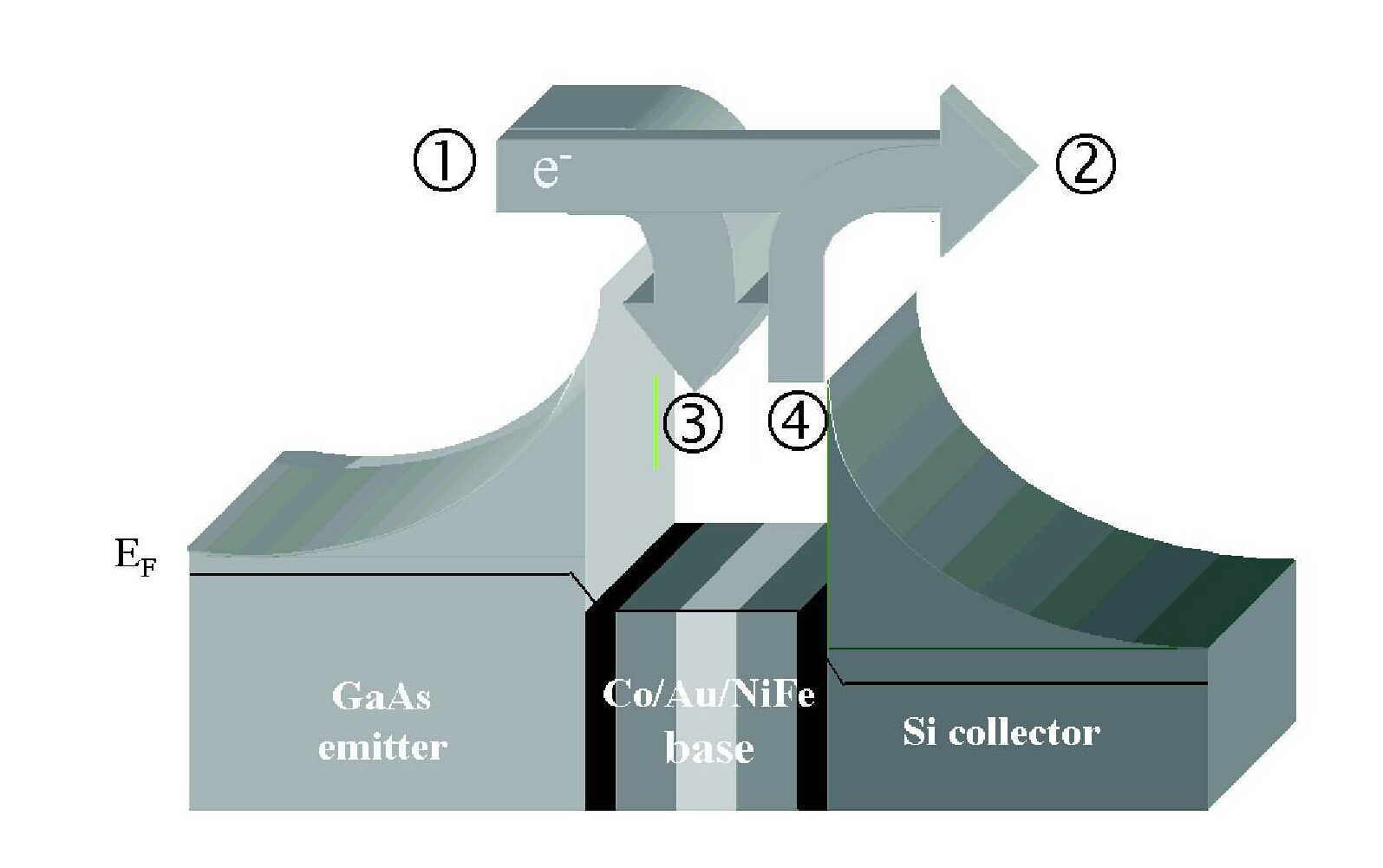
One way to achieve this structure is to join the two semiconductor substrates constituting the emitter and collector of the transistor structure. This SVT does not rely on spin-dependent transport in the semiconductor, but builds on the spin-scattering of hot electrons in metallic layers. Scattering of hot electrons is not yet well understood. The transfer coefficient (a), defined as the ratio of the collected current to the injected current, is of the order of 10-4% and hence seriously limits the applicability of the device. Enhancement of the Schottky barrier height at the collector improves a and reduces leakage current. IMEC obtained good results by growing an AlAs (2 nm)/GaAs (4nm) periodic structure on top of a lowly-doped emitter layer, resulting in a quantum-well structure. After implementation of such an emitter in a SVT, we improved a by 10-2%. |
Schematic representation of a GaAs/Si spin-valve transistor, indicating the different electrical current components determining its operation. Source: IMEC. Click image for larger version. |
To make new spintronic components a reality, research must address three different problem areas. One is the creation of a spin-ensemble in a semiconductor. This "spin-injection" involves creating a situation with majority and minority spins. A second problem is external control over the spin-packet movement, coherence and lifetime on a (sub-)micron scale in the time frame of nano- to microseconds. The third problem is the external observation of a discernible spintronic effect that could be used to interpret or 'read' the outcome of a spintronic device function.
How to inject electrons with definite spin? In a research environment, spin-polarized electrons are often optically generated using circularly polarized light. However, for spintronics, one would prefer an all-electrical source. Alternatives are: (a) a diffusive Ohmic contact; (b) 100% polarized injectors, such as half-metals; (c) tunnel injectors and (d) a (buried) magnetic semiconductor structure as spin-filter or spin-injector. The discussion below is focused on IMEC's recent results in the development of a half-metallic spin-source, a tunnel-barrier spin-source and the use of magnetic semiconductors.
Half-metallic ferromagnets such as NiMnSb can be grown epitaxially on GaAs(100) and (111). NiMnSb is half-metallic in the bulk. It has, however, been much more difficult to establish a high degree of spin-polarization at the surface of NiMnSb thin films. A key issue here is to have well-controlled surfaces. For the injection of spin-polarized carriers into a semiconductor, not the top surface but the bottom interface of the ferromagnetic material is important. It is crucial to obtain a high crystal quality from the initial nucleation phase on. The crystal structure of NiMnSb is very closely related to the zincblende structure of III-V semiconductors, making the NiMnSb/GaAs combination a very good candidate for atomically controlled interfaces. A typical sample consists in a 200nm GaAs buffer and 260 to 350nm thick NiMnSb films. These structures are currently being incorporated in spin-injection structures to evaluate their high (close to 100%) spin-polarization.
The problems associated with the metal/semiconductor interface can be circumvented by incorporating a high density of magnetic impurities (such as Mn) into the III-V semiconductor to obtain a (ferro)magnetic semiconductor such as GaMnAs. Although the exact nature of the magnetism is still under intense study, researchers have obtained moderate spin-injection efficiencies using GaMnAs as a spin-injector. One of the challenges is to incorporate the magnetic structures in semiconductor heterostructures such that the spintronic properties of GaMnAs can be exploited.
An alternative approach is to use a tunnel-barrier spin-injector, based on existing expertise in the fabrication of magnetic tunnel junctions. Here, the magnetic properties can be well controlled at the metal/insulator interface. This interface will be more stable over time and will be less sensitive to temperature changes than direct metal/semiconductor heterostructures.
|
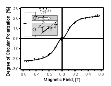
Degree of circular polarization of the spin-LED with magnetic metal/Al2O3 tunnel barrier contact (80K). Source: IMEC. Click for larger version. |
IMEC has measured the spin-polarized current injection of such a structure through its optical response. For this purpose, we fabricated a tunnel contact spin-LED, consisting of a GaAs-based light-emitting device structure using a ferromagnetic metal. The magnetic contact (CoFe/NiFe) injects spin-polarized current through an Al2O3 barrier in the active region of the LED. The optical selection rules in GaAs lead to the generation of circularly polarized light, which is analyzed to measure the degree of spin-injection. This measurement approach unambiguously shows the signature of spin-injection. With these injector structures, spin-injection at room temperature is possible using a standard metal/insulator/semiconductor technology. The injection efficiency of the first devices was above 8% (80K). |
In addition to the near-term studies of spin-transport properties of semiconductors, there is a lot of enthusiasm for a long-term and more ambitious application of the electron spin: quantum computation, where spins are a very promising quantum-effect to deal with. The spins of the electrons (and spin-½ nuclei) are good candidates for qubits or quantum bits, one of the three cornerstones of future quantum computers. The requirements for such application area are still under discussion.
The use of the electron spin in semiconductor devices is an increasingly active area of research. Recently, a breakthrough has been realized in the area of spin-injection, the problem of injecting spin-polarized current in a semiconductor.
However, the spintronics field requires a shift in thinking about computing as we know it today. Making spintronic devices a reality requires a substantial amount of fundamental materials development, together with the experimental characterization of spin properties in complex heterostructures. Only then can the additional functionality of spintronic devices be evaluated. The key question will be whether any potential benefit of such technology will be worth the production costs.
Jo De Boeck (PhD) heads the magnetoelectronics group at IMEC, Leuven. He joined IMEC in 1986 and he has been active in the magnetoelectronics and spintronics area since 1992. He is part-time professor at the TU Delft, which is 'Technische Universiteit Delft', or, in English, Delft University of Technology.
Mieke Van Bavel received the Ph.D. degree in physics in 1995. She joined IMEC in 2001 as a scientific editor and is jointly responsible for authoring and editing the research organization's numerous company technical documents and publications.
| This article is Copyright ©2002 by IMEC, Leuven, Belgium. Used by permission. |
| This site is Copyright ©2001-2002 by Thin Film Manufacturing. All Rights Reserved |