| thinfilmmfg.com
|
Silicon dominates microelectromechanical systems (MEMS) research, and for good reason. It has excellent electronic and mechanical properties. Furthermore, thanks to the integrated circuit industry, a large body of silicon manufacturing expertise already exists. Silicon MEMS are especially appealing for integration with microelectronics.
Even so, silicon microdevices have been slow to emerge from R&D labs into the commercial marketplace. Robust, reliable MEMS manufacturing remains elusive. For example, adhesion between moving parts and each other or the underlying substrate remains a serious problem. As Roya Maboudian, from the University of California Berkeley's Chemical Engineering Department, explained at last week's Materials Research Society workshop on MEMS materials issues, adhesion can occur during both manufacturing and device use.
| Manufacturing adhesion usually happens during the release step. Surface micromachining builds structures one layer at a time by depositing alternating layers of silicon dioxide and polysilicon. Conventional lithography processes sculpt the polysilicon to form beams, gears, and other mechanical elements. Finally, an etch step removes the silicon dioxide layers, releasing the moving parts. Surface micromachining can build extremely complicated multilayer structures. |
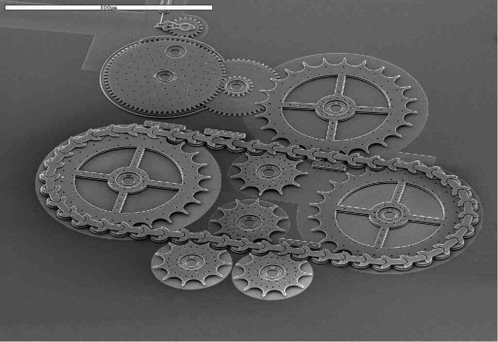
Sandia National Laboratories' Summit V process can produce unsupported spans as long as 500 microns. Click image for larger version. Image courtesy of Sandia National Laboratories. |
Unfortunately, the HF etch usually used for the release step leaves a hydrophilic surface behind. Rinse water wets the surface, so that surface tension pulls parts together. The Berkeley group measured adhesion in an array of cantilevered beams of various lengths. They found that beams more than 100 microns long adhered to the substrate during the release etch.
Release adhesion has plagued MEMS manufacturing for years, but no completely satisfactory solution has yet been found. Supercritical CO2 drying tends to leave particulates behind, Maboudian said, while using an HF vapor release etch limits designers to a narrow range of compatible materials. Furthermore, moving parts can adhere in use even if the release etch succeeds. Electrostatic forces between the parts, including van der Waals forces and hydrogen bonds, drive in-use adhesion. To prevent it, the Berkeley group explored a variety of self-assembled monolayer (SAM) coatings, including per-fluoro-alkyl-trichlorosilane SAMs and alkene-based molecular films. These coatings create hydrogen-terminated hydrophobic surfaces, reducing release adhesion. They also increase the work of adhesion by up to four orders of magnitude, thereby helping to prevent in-use adhesion.
As surface micromachined structures become more complex, the residual stresses incorporated in each layer of polysilicon become more important. Depending on growth conditions, the resulting film structure can vary from 0.1 micron grains under tensile stress to large, columnar grains under compressive stress. As Arthur Heuer, of the Materials Science and Engineering Department at Case Western Reserve explained, annealing above 1000°C relaxes these residual stresses but is undesirable when the substrate also includes integrated circuits. Instead, Heuer described a multilayer polysilicon process. By varying the deposition conditions for each layer, the Case Western Reserve group produced films with near-zero overall stresses, as well as films with controlled curvature.
Though silicon is a good material, it is not perfect for all applications. SiC, for example, is electronically and mechanically stable at temperatures above 500°C, is chemically stable, and is highly wear resistant. Because it is chemically stable, however, SiC is very difficult to pattern. Reactive ion etching (RIE) of SiC is not selective enough to allow multilayer processes analogous to those used for polysilicon MEMS.
Mehran Mehregany and Christian Zorman, both in the Department of Electrical Engineering and Computer Science at Case Western Reserve, proposed two different approaches to surface micromachining of SiC. The first method, which resembles the copper damascene process used for integrated circuit interconnects, deposits poly-SiC into polysilicon mold structures, then mechanically polishes away excess SiC to expose the top of the mold. Potassium hydroxide and HF etchants remove the polysilicon mold and the SiO2 release layer, respectively. This method may offer an alternative to RIE for a range of materials.
The second method examined by Mehregany and Zorman focuses on the quality of the initial SiC substrate. Lattice and thermal mismatches produce many crystalline defects in 3C-SiC films grown on Si wafers. These defects compromise electronic device performance. Research has focused on SiC-on-insulator films because SiO2 matches SiC more closely. The Case Western Reserve approach begins with deposition of a SiC layer on a silicon wafer, followed by a thin SiO2 layer and a thick polysilicon film. Complete etching of the original wafer leaves behind a SiC/SiO2/polysilicon structure. Additional SiC grown on this wafer offers a suitable substrate for surface micromachining, and possibly for device fabrication as well.
Of course, many MEMS applications require properties that no silicon compound can offer. Actuators made from shape memory alloys like TiNi offer relatively long actuation distances, due to their large recoverable strains, and have actuation work densities up to 50 MJ/m3. These actuators can open and close microvalves against high pressures and allow wider openings and larger flow rates.
Piezoelectric materials like lead zirconate titanate (PZT) couple electrical and mechanical energy. Magnetic materials can be manipulated by magnetic fields. Accordingly, both classes of materials can serve as sensors and actuators in MEMS structures. Magnetic materials have a further advantage in that they can draw upon fabrication technologies developed for the magnetic recording industry.
As the workshop showed, the list of potential materials for MEMS devices is increasing steadily. Unfortunately, as Exponent Principal Engineer Stuart Brown explained, very little is known about the behavior of any of these materials on the microscale. The effects of scale on crack growth, fatigue, and wear are essentially unknown. Calibration standards, standard test structures, and standard measurement techniques do not exist. These knowledge gaps, Brown said, offer great opportunities for research, but present great risk for manufacturers.
| This site is Copyright ©2001-2002 by Thin Film Manufacturing. All Rights Reserved |