| thinfilmmfg.com
|
For years, lithographers have grabbed headlines and earned the admiration of their peers by laughing at the laws of optics. Again and again, pundits predicting the end of optical lithography have been proven wrong by new light sources, exotic optic, and other resolution enhancements. Lithographic technologies always seem able to print smaller feature sizes than originally seemed possible. Switching to a smaller exposure wavelength requires an enormous investment in new steppers, new resist processes, and process integration. Fab managers are reluctant to make that investment when resolution enhancements can squeeze comparable results from existing equipment.
But are the results really comparable? Is it really possible to break the laws of optics indefinitely? As it turns out, two factors tilt the scales away from resolution enhancements and toward shorter exposure wavelengths: manufacturability and cost.
Manufacturability is roughly defined by the k1 parameter from the Rayleigh criterion. Larger numerical apertures reduce depth of focus, requiring extremely tight wafer flatness and backside cleanliness specifications. As CD shrinks at maximum NA (about 0.8) and fixed wavelength, k1 goes down as well. It is not yet clear whether processes with k1 values less than 0.25 will be viable for volume production.
| Manufacturability is roughly defined by the k1 parameter from the Rayleigh criterion. Larger numerical apertures reduce depth of focus, requiring extremely tight wafer flatness and backside cleanliness specifications. As CD shrinks at maximum NA (about 0.8) and fixed wavelength, k1 goes down as well. It is not yet clear whether processes with k1 values less than 0.25 will be viable for volume production. |
|
|
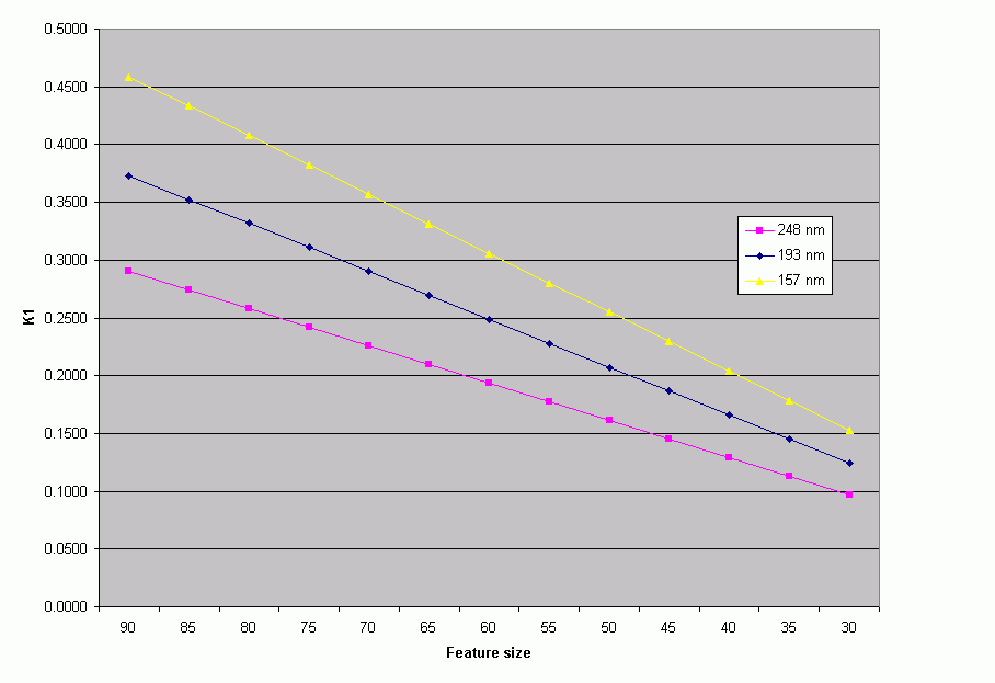
The k1 parameter declines with feature size, putting more and more pressure on resolution budgets. Reducing the wavelength eases the pressure, but only temporarily. Feature size in nanometers, NA = 0.8. Click image for larger version. |
Such extreme sub-wavelength lithography is only possible with
extensive use of optical proximity correction (OPC) and phase shift masks
(PSM). OPC works by adding assist features to the mask. These features compensate
for line shortening, corner rounding, and other distortions caused by sub-wavelength
features. Phase shift masks correct more serious distortions by shifting
some light out of phase as it passes through the mask. Destructive interference
between adjacent shifted and unshifted regions blanks out dark regions of
the aerial image, sharpening the edges of light regions.
Both OPC and PSM add significant complexity and cost to the photomask. OPC assist features are smaller than the nominal mask design rule, making these features much more difficult to write and inspect. PSM masks have three layers (shifted, not shifted, and chrome) rather than the usual two (glass and chrome). In some designs, the phase shift layer requires precise etching of the quartz blank. The mask, once a low margin commodity, becomes a critical and expensive piece of process tooling. At some point, the mask cost becomes a significant fraction of the total lithography process cost. |
Researchers at SEMATECH have studied lithography costs to determine the cost/benefit tradeoff between resolution-enhanced masks and shorter exposure wavelengths. A group led by Ed Muzio found that the four main drivers of lithography cost of ownership are mask usage, mask cost, tool cost, and tool throughput.
Mask usage-the number of wafers printed with a given mask-follows a bimodal distribution, SEMATECH found. DRAM and microprocessor manufacturers tend to cluster around the high usage peak, averaging about 8000 wafers per mask (WPM). ASIC and logic suppliers tend to cluster around the low usage peak, averaging about 500 WPM. Low mask usage applications are much more sensitive to mask cost. Above about 2000 WPM, the lithography COO approaches a constant value, regardless of mask usage.
Mask cost, in turn, increases with the complexity of the mask. SEMATECH found that the mask write step, including both capital costs and write time, accounts for fully 50% of total mask cost. As Ken Rygler of Dupont Photomasks noted, mask writers have not achieved the consistent productivity improvement that the rest of the semiconductor manufacturing industry has come to expect. Improvements in mask throughput would significantly lower mask costs.
Mask yield and mask blanks are also important contributors. Yield of enhanced masks can be very low, wasting valuable mask writer throughput and also destroying expensive mask blanks.
Dual exposures are one possible solution to the mask cost problem. This method uses a conventional binary mask to pattern larger features on the gate level. A second exposure with a dark field phase shift mask trims the minimum geometry features to the desired size. The limited use of phase shifting within the design simplifies the mask, reducing costs. Unfortunately, this approach also halves the critical layer throughput.
SEMATECH found that neither low nor high mask usage applications could justify the double exposure approach on COO grounds. If this approach proves viable, it will be because it offers a yield or device performance benefit.
Throughput sensitivity levels off at around 40 wafers per hour (WPH). Cost continues to decline at higher throughputs, though less dramatically. High throughput tools also reduce the impact of tool cost.
The speed of current resists for 193 nm and 157 nm lithography, combined with the limited exposure dose available from 193 nm and 157 nm lasers, reduces the theoretical maximum throughput at these wavelengths.
The final key COO parameter, tool cost, has been climbing at an exponential rate for several decades. Exposure systems cost about US$1 million in the mid-1980s, while some current systems have reached US$10 million. SEMATECH predicts that competitive pressures will slow this climb. The Muzio study expects tool costs for the period through 2007 to grow more slowly than the long term trend.
SEMATECH also notes that many applications do not need the full exposure field sizes available on most steppers. Reducing the exposure field reduces the lens cost substantially: it is easier to maintain a given image resolution over a smaller area. High NA systems with smaller fields might see as much as a factor of 2.6 reduction in lens costs.
Overall, SEMATECH found that low mask usage applications are most sensitive to mask costs, while high mask usage applications are most sensitive to tool cost and throughput. At the 100 nm node, the differences are significant enough to affect the economic justification for smaller wavelength steppers.
COO Analysis for 100 nm node with 300 mm wafers.
| Technology | Reticle | Tool | WPH | COO 500 WPM | COO 8000 WPM |
| 193 nm Alt. PSM | US$28K | US$11M | 38.9 | US$89 | US$33 |
| 157 nm binary w/OPC | US$23K | US$14M | 38.9 | US$83 | US$37 |
Source: SEMATECH
| This site is Copyright ©2001 by Thin Film Manufacturing. All Rights Reserved |